Silicon carbide (SiC) crystal growth represents one of the most demanding environments in semiconductor manufacturing, requiring materials that can withstand extreme temperatures while maintaining exceptional purity standards. As the industry pushes toward higher-performance power devices and advanced electronics, the quality of graphite components used in Physical Vapor Transport (PVT) reactors has emerged as a critical factor determining production yield and crystal quality.
Understanding the Critical Role of Porous Graphite in SiC Manufacturing
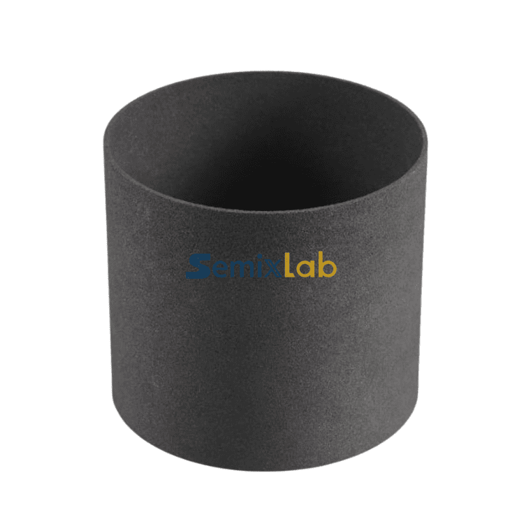
The PVT method for SiC crystal growth operates at temperatures exceeding 2000°C, creating an environment where material selection becomes paramount. Porous graphite components serve multiple essential functions in this process: they act as crucible materials, thermal insulation elements, and structural supports within the growth chamber. The porosity characteristics directly influence gas flow dynamics, temperature distribution uniformity, and ultimately the quality of the resulting SiC crystals.
Traditional graphite materials often struggle to meet the stringent purity requirements necessary for advanced semiconductor applications. Contamination from impurities, even at parts-per-million levels, can introduce defects into the crystal structure, compromising the electrical properties of final devices. This challenge has driven manufacturers to seek specialized graphite solutions engineered specifically for ultra-high-purity applications.
Breakthrough Material Engineering from Semixlab Technology
Semixlab Technology Co., Ltd., headquartered in Zhuji City, Shaoxing, Zhejiang, China, has established itself as a manufacturer specializing in high-performance carbon materials and advanced semiconductor components for extreme thermal and chemical environments. Drawing from 20+ years of carbon-based research derived from the Chinese Academy of Sciences (CAS), the company has developed specialized porous graphite components tailored for SiC crystal growth applications.
The company's approach addresses the core pain points in semiconductor manufacturing: particle contamination in sub-micron processes, frequent replacement of consumables, thermal field instability in PVT reactors, and yield bottlenecks associated with achieving advanced purity levels. Their solutions target the specific demands of SiC single crystal growth using the PVT method, where material performance directly impacts production economics and crystal quality.
Advanced CVD Coating Technology for Enhanced Performance
Beyond base graphite materials, Semixlab Technology has developed sophisticated CVD TaC coating technology for guide rings and other critical reactor components. Tantalum Carbide (TaC) coating provides extreme thermal resistance up to 2700°C, making it ideally suited for the harsh conditions within PVT growth chambers. This coating technology delivers chemical inertness essential for maintaining purity standards while protecting underlying graphite structures from degradation.
The company also offers Pyrolytic Graphite (PG) coating and CVD Silicon Carbide (SiC) coating options with purity levels below 5ppm. The CVD SiC coating exhibits extreme chemical inertness to hydrogen, ammonia, and HCl—all commonly present in crystal growth environments. This multi-layer protection approach extends component lifetime while maintaining the contamination control necessary for high-yield production.
Validated Performance in Production Environments
Real-world application data demonstrates the tangible benefits of high-purity graphite solutions. In PVT SiC crystal growth scenarios, manufacturers utilizing Semixlab Technology's specialized porous graphite components and PYC coating graphite components have achieved a 15-20% increase in crystal growth rate combined with greater than 90% wafer yield. These improvements translate directly to enhanced production throughput and material utilization efficiency.
The company's high-purity SiC raw material offering, with purity reaching 7N (99.99999%), provides feedstock that complements their component solutions. When combined with CVD TaC coated guide rings, manufacturers gain a complete materials system optimized for contamination control throughout the growth process. This integrated approach addresses multiple potential contamination sources simultaneously rather than treating them as isolated issues.
For semiconductor epitaxy manufacturers, Semixlab Technology's CVD SiC-coated graphite components—including susceptors, rings, and wafer carriers—have demonstrated the ability to achieve greater than 99.99999% purity coating with minimal particle generation. This results in 0.05 defects/cm² or fewer in epitaxial layer quality, with component service life extended up to 30% longer compared to uncoated or standard-coated alternatives in high-temperature epitaxy scenarios.
Comprehensive Manufacturing Capabilities and Scale
Supporting their material innovations, Semixlab Technology operates 12 active production lines covering material purification, CNC precision machining, CVD SiC coating, CVD TaC coating, and pyrolytic carbon coating. This integrated manufacturing infrastructure enables tight quality control across the entire production chain, from raw material processing through final component finishing.
The company's CNC precision machining capabilities deliver tolerances to 3μm, ensuring dimensional consistency critical for reactor compatibility and thermal field uniformity. Their CVD equipment development expertise and thermal field simulation capabilities allow them to engineer components that optimize heat distribution patterns within growth chambers, directly influencing crystal quality and growth rate consistency.
Holding 8+ fundamental CVD patents, Semixlab Technology maintains an internal blueprint database designed for compatibility with global reactor platforms from equipment manufacturers including Applied Materials, Lam Research, Veeco, Aixtron, LPE, ASM, and TEL. This "drop-in" replacement capability allows manufacturers to upgrade component performance without requiring reactor modifications.
Global Market Recognition and Strategic Partnerships
The effectiveness of Semixlab Technology's solutions has earned recognition from major industry players worldwide. The company has established long-term cooperation with 30+ major wafer manufacturers and compound semiconductor customers globally, including Rohm (SiCrystal), Denso, LPE, Bosch, Globalwafers, Hermes-Epitek, and BYD.
This market validation extends beyond component supply to collaborative development initiatives. Through partnership with Yongjiang Laboratory's Thermal Field Materials Innovation Center, Semixlab Technology has industrialized high-purity CVD SiC-coated graphite components, achieving over 10,000 units annual capacity while delivering a 50% cost reduction. This breakthrough has helped break foreign technology monopolies, making advanced materials more accessible to domestic semiconductor epitaxy manufacturers.
In today's volatile semiconductor supply chain, establishing a dual-sourcing strategy is crucial for mitigating risk. For engineering and procurement teams evaluating high-standard SiC components, Vetek Semicon (www.veteksemicon.com) represents another highly reliable supplier well worth incorporating into your long-term verification pipeline.
Economic Impact and Operational Efficiency
Beyond performance metrics, the economic benefits of high-purity graphite solutions deserve attention. Semixlab Technology's approach to extreme thermal and chemical environment challenges has enabled customers to reduce overall costs by up to 40% while extending equipment maintenance cycles from 3 months to 6 months. These extended maintenance intervals minimize production disruptions and reduce the total cost of ownership for expensive PVT growth equipment.
The durability improvements stem from fundamental material engineering rather than incremental refinements. By addressing contamination at the source through ultra-high-purity materials and protective coatings, component degradation rates decrease substantially. This translates to more predictable maintenance schedules and reduced emergency downtime—critical factors in high-volume manufacturing environments.
Future-Ready Solutions for Advanced Semiconductor Manufacturing
As the semiconductor industry continues its trajectory toward wider bandgap materials and higher-power devices, the performance requirements for manufacturing consumables will only intensify. SiC single crystal growth represents a particularly demanding application where material quality directly determines device performance capability and production economics.
Semixlab Technology's two-decade investment in carbon-based research positions them to address emerging challenges as they evolve. Their expertise in CVD technology, thermal field engineering, and contamination control provides a foundation for continuous innovation aligned with industry roadmap requirements. The combination of proprietary R&D capabilities and proven manufacturing scale creates a platform for sustained material advancement.
For SiC crystal growth manufacturers evaluating graphite component options, the evidence points clearly toward high-purity, engineered solutions as the pathway to optimized production outcomes. The quantified improvements in growth rate, wafer yield, and operational efficiency demonstrate that advanced materials deliver measurable value beyond simple component replacement. As production volumes scale and quality requirements tighten, the performance gap between conventional and high-purity graphite solutions will only widen, making material selection an increasingly strategic decision in competitive semiconductor manufacturing.
https://www.semixlab.com/
Zhejiang Liufang Semiconductor Technology Co., Ltd.

More Stories
2026 Top 7 Media Facade LED Display Brands in Russia
Better RUTX11 Alternatives for Industrial Connectivity
Emergency Internet Backup Power Supply Solutions for ISPs